
The OpenOCD Option
OpenOCD (on chip debugger) is not very intuitive, and it’s the kind of tool that if you’ve not used it for a while.. you have to restart from scratch!
It comes with a collection of supported devices, but out of the box, the AT91SAM9G25 is not one of those. Thanks to the author of this blog, he published a configuration file for our chip and OpenOCD: https://jopee.wordpress.com/6lowpan-gateway/
Here is the file, all credits goes to the author of the blog.
################################
# Target:    Atmel AT91SAM9G25
######################################
if { [info exists CHIPNAME] } {
set AT91_CHIPNAME $CHIPNAME
} else {
set AT91_CHIPNAME at91sam9g25
}
source [find target/at91sam9.cfg]
# Set fallback clock to 1/6 of worst-case clock speed (which would be the 32.768 kHz slow clock).
adapter_khz 5
# Establish internal SRAM memory work areas that are important to pre-bootstrap loaders, etc.  The
# AT91SAM9G25 has one 32kByte SRAM area, starting at 0x00300000.
$_TARGETNAME configure -work-area-phys 0x00300000 -work-area-size 0x8000 -work-area-backup 1
set _FLASHTYPE nandflash_cs3
# Set reset type.  Note that the AT91SAM9G20-EK board has the trst signal disconnected.  Therefore
# the reset needs to be configured for “srst_only”.  If for some reason, a zero-ohm jumper is
# added to the board to connect the trst signal, then this parameter may need to be changed.
reset_config srst_only
adapter_nsrst_delay 200
jtag_ntrst_delay 200
# If you don’t want to execute built-in boot rom code (and there are good reasons at times not to do that) in the
# AT91SAM9 family, the microcontroller is a lump on a log without initialization.  Because this family has
# some powerful features, we want to have a special function that handles “reset init”.  To do this we declare
# an event handler where these special activities can take place.
scan_chain
$_TARGETNAME configure -event reset-init {at91sam9g25_reset_init}
$_TARGETNAME configure -event reset-start {at91sam9g25_reset_start}
# NandFlash configuration and definition
nand device nandflash_cs3 at91sam9 $_TARGETNAME 0x40000000 0xffffe014
at91sam9 cle 0 22
at91sam9 ale 0 21
at91sam9 rdy_busy 0 0xfffff800 5
at91sam9 ce 0 0xfffffA00 4
proc read_register {register} {
        set result “”
        mem2array result 32 $register 1
        return $result(0)
}
proc at91sam9g25_reset_start { } {
# Make sure that the the jtag is running slow, since there are a number of different ways the board
# can be configured coming into this state that can cause communication problems with the jtag
# adapter.  Also since this call can be made following a “reset init” where fast memory accesses
# are enabled, need to temporarily shut this down so that the RSTC_MR register can be written at slower
# jtag speed without causing GDB keep alive problem.
arm7_9 fast_memory_access disable
adapter_khz 2                   ;# Slow-speed oscillator enabled at reset, so run jtag speed slow.
halt                            ;# Make sure processor is halted, or error will result in following steps.
wait_halt 10000
#mww 0xfffffe08 0xa5000001       ;# RSTC_MR : enable user reset.
#mww 0xFFFFFE00 0xA500000B ;# Reset CPU
}
proc at91sam9g25_reset_init { } {
mww 0xfffffe44 0x00008000 ;# WDT_MR : disable watchdog.
# Enable the main 12 MHz oscillator in CKGR_MOR register.
# Wait for MOSCS in PMC_SR to assert indicating oscillator is again stable after change to CKGR_MOR.
mww 0xfffffc20 0x01370F01
while { [expr [read_register 0xfffffc68] & 0x01] != 1 } { sleep 1 }
echo 1
## PMC Clock generator PLLA register
# DIVA = 3
# PLLACOUNT = 0x3F
# MULA = 0xc7
# OUTA = 0
# PLLA Frequency = 12 MHz / DIVA * (MULA + 1) = 800MHz
mww 0xfffffc28 0x20C73f03
while { [expr [read_register 0xfffffc68] & 0x02] != 2 } { sleep 1 }
echo 2
        mww 0xfffffc30 0x00001300
        while { [expr [read_register 0xfffffc68] & 0x08] != 8 } { sleep 1 }
echo 3
# Set master system clock prescaler divide by 6 and processor clock divide by 2 in PMC_MCKR.
# Wait for MCKRDY signal from PMC_SR to assert.
# System Clock = 800 MHz / 6 = 133MHz
# CPU Clock = 800 MHz / 2 = 400 MHz
#
mww 0xfffffc30 0x00001302
while { [expr [read_register 0xfffffc68] & 0x08] != 8 } { sleep 1 }
echo 4
# Switch over to adaptive clocking.
adapter_khz 100000
# Enable faster DCC downloads and memory accesses.
arm7_9 dcc_downloads enable
arm7_9 fast_memory_access enable
### Configure NAND
#
mww 0xFFFFFA04 0xffffffff
mww 0xfffffa74 0x3fef
mww 0xfffffc10 0x00000008
mww 0xfffffa00 0x00000030
mww 0xfffffa10 0x00000010
mww 0xfffffa30 0x00000010
mww 0xFFFFEA30 0x00020002
mww 0xFFFFEA34 0x04040404
mww 0xFFFFEA38 0x00070007
mww 0xFFFFEA3c 0x00030003
# configure NAND PMECC
### DRAM Setup
#
#
#
# CCFG_EBICSA
# Configure DRAM on EBI CS 1
# Set low drive strength
mww 0xFFFFDF20 0x0102000A
        # 0. Enable DDR2 Clock
        mww 0xfffffc00 0x4
# DDRSDRC_HS
# Disable Anticipated read access
mww 0xffffe82c 0x04
# DDRSDRC_MD
# 16-bit databus
# DDR-2
# According to the datasheet this value SHOULD be 0x14 for 16-bit DDR2!
mww 0xffffe820 0x16
# DDRSDRC_CR
#
# 10 col bits
# 13 row bits
# CAS 3
mww 0xffffe808 0x100039
## DDRSDRC_TPR0
#
mww 0xffffe80c 0x21222226
## DDRSDRC_TPR1
#
mww 0xffffe810 0x2c81312
## DDRSDRC_TPR2
#
mww 0xffffe814 0x1372
## DDRSDRC_MR
mww 0xffffe800 0x01 ;# NOP
mww 0x20000000 0x00
sleep 1
mww 0xffffe800 0x01 ;# NOP
mww 0x20000000 0x00
mww 0xffffe800 0x02 ;# All banks pre-charge
mww 0x20000000 0x00
mww 0xffffe800 0x05 ;# Extended load mode register
mww 0x24000000 0x00
mww 0xffffe800 0x05 ;# Extended load mode register
mww 0x26000000 0x00
mww 0xffffe800 0x05 ;# Extended load mode register
mww 0x22000000 0x00
## DDRSDRC_CR
mww 0xffffe808 0x1000b9
# Reset DLL
mww 0xffffe800 0x03 ;# LMR
mww 0x20000000 0x00
mww 0xffffe800 0x02 ;# All banks pre-charge
mww 0x20000000 0x00
mww 0xffffe800 0x04 ;# Auto refresh
mww 0x20000000 0x00
mww 0xffffe800 0x04 ;# Auto refresh
mww 0x20000000 0x00
        # DDRSDRC_CR
        #
        # 10 col bits
        # 13 row bits
        # CAS 3
        mww 0xffffe808 0x100039
       mww 0xffffe800 0x03 ;# LMR
        mww 0x20000000 0x00
        mww 0xffffe808 0x100739
       mww 0xffffe800 0x05 ;# eLMR
        mww 0x22000000 0x00
        mww 0xffffe808 0x100039
       mww 0xffffe800 0x05 ;# eLMR
        mww 0x26000000 0x00
       mww 0xffffe800 0x00 ;# Normal
        mww 0x20000000 0x00
## DDRSDRC_RTR
mww 0xffffe804 0x411
mww 0xffffe82c 0x04
sleep 1
mww 0x20000000 0xdeadbeef
mdw 0x20000000
nand probe 0
}
Save this file in /usr/share/openocd/scripts/board/at91sam9g25.cfg
Now, you need to create an openocd.cfg file, describing your setup, which is mainly:
- your probe
- the board
- your own routines
I’ll not go through all the steps to create the file – it took me a while! Find below the content of the file I used.
# Use JLink interface (/usr/share/openocd/scripts/interface/jlink.cfg)
source [find interface/jlink.cfg]

# JLink requires a speed to be used by the probe. 0 means adaptive.
adapter_khz 0

# JLink also requires to specify the transport type. Here we use JTAG
transport select jtag

# Load the board config file for the at91
source [find board/at91sam9g25.cfg]

# My own initialization routine. Reset the device, and configure the NAND bank for access.
proc reset_ben {} {
 reset halt
 adapter_khz 0

 # Configure NAND

 mww 0xFFFFFA04 0xffffffff
 mww 0xfffffa74 0x3fef
 mww 0xfffffc10 0x00000008
 mww 0xfffffa00 0x00000030
 mww 0xfffffa10 0x00000010
 mww 0xfffffa30 0x00000010
 mww 0xFFFFEA30 0x00020002
 mww 0xFFFFEA34 0x04040404
 mww 0xFFFFEA38 0x00070007
 mww 0xFFFFEA3c 0x00030003

 # Configure NAND PMECC
 ### DRAM Setup

 # CCFG_EBICSA
 # Configure DRAM on EBI CS 1
 # Set low drive strength
 mww 0xFFFFDF20 0x0102000A
 # 0. Enable DDR2 Clock
 mww 0xfffffc00 0x4

 # DDRSDRC_HS
 # Disable Anticipated read access
 mww 0xffffe82c 0x04

 # DDRSDRC_MD
 # 16-bit databus
 # DDR-2
 # According to the datasheet this value SHOULD be 0x14 for 16-bit DDR2!
 mww 0xffffe820 0x16
 # DDRSDRC_CR
 #
 # 10 col bits
 # 13 row bits
 # CAS 3
 mww 0xffffe808 0x100039
 # DDRSDRC_TPR0
 mww 0xffffe80c 0x21222226
 # DDRSDRC_TPR1
 mww 0xffffe810 0x2c81312
 # DDRSDRC_TPR2
 mww 0xffffe814 0x1372
 # DDRSDRC_MR
 mww 0xffffe800 0x01 ;# NOP
 mww 0x20000000 0x00
 sleep 1
 mww 0xffffe800 0x01 ;# NOP
 mww 0x20000000 0x00
 mww 0xffffe800 0x02 ;# All banks pre-charge
 mww 0x20000000 0x00
 mww 0xffffe800 0x05 ;# Extended load mode register
 mww 0x24000000 0x00
 mww 0xffffe800 0x05 ;# Extended load mode register
 mww 0x26000000 0x00
 mww 0xffffe800 0x05 ;# Extended load mode register
 mww 0x22000000 0x00
 # DDRSDRC_CR
 mww 0xffffe808 0x1000b9
 # Reset DLL
 mww 0xffffe800 0x03 ;# LMR
 mww 0x20000000 0x00
 mww 0xffffe800 0x02 ;# All banks pre-charge
 mww 0x20000000 0x00
 mww 0xffffe800 0x04 ;# Auto refresh
 mww 0x20000000 0x00
 mww 0xffffe800 0x04 ;# Auto refresh
 mww 0x20000000 0x00

 # DDRSDRC_CR
 #
 # 10 col bits
 # 13 row bits
 # CAS 3
 mww 0xffffe808 0x100039
 mww 0xffffe800 0x03 ;# LMR
 mww 0x20000000 0x00
 mww 0xffffe808 0x100739
 mww 0xffffe800 0x05 ;# eLMR
 mww 0x22000000 0x00
 mww 0xffffe808 0x100039
 mww 0xffffe800 0x05 ;# eLMR
 mww 0x26000000 0x00
 mww 0xffffe800 0x00 ;# Normal
 mww 0x20000000 0x00

 # DDRSDRC_RTR
 mww 0xffffe804 0x411
 mww 0xffffe82c 0x04
 sleep 1
 mww 0x20000000 0xdeadbeef
 mdw 0x20000000
 nand probe 0
}
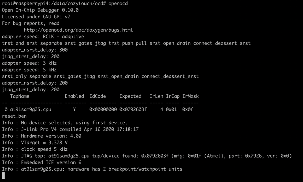
You can now simply start openocd. If everything goes right, you should see something like this:
You can now interact with OpenOCD, telnetting to the local port 4444, and start with my routine “reset_ben”:
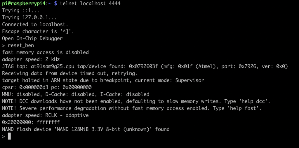
The NAND flash device has been found and identified correctly. Great! We can now start dumping the NAND. For memory, here is the list of available NAND commands:
nand
      NAND flash command group (command valid any time)
  nand check_bad_blocks bank_id [offset length]
        check all or part of NAND flash device for bad blocks
  nand device bank_id driver target [driver_options ...]
        defines a new NAND bank (configuration command)
  nand drivers
        lists available NAND drivers (command valid any time)
  nand dump bank_id filename offset length ['oob_raw'|'oob_only']
        dump from NAND flash device
  nand erase bank_id [offset length]
        erase all or subset of blocks on NAND flash device
  nand info [banknum | first_bank_num last_bank_num]
        print info about one or more NAND flash devices
  nand init
        initialize NAND devices (configuration command)
  nand list
        list configured NAND flash devices
  nand probe bank_id
        identify NAND flash device
  nand raw_access bank_id ['enable'|'disable']
        raw access to NAND flash device
  nand verify bank_id filename offset
            ['oob_raw'|'oob_only'|'oob_softecc'|'oob_softecc_kw']
        verify NAND flash device
  nand write bank_id filename offset
            ['oob_raw'|'oob_only'|'oob_softecc'|'oob_softecc_kw']
        write to NAND flash device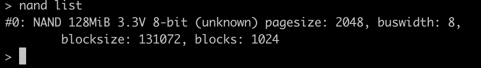
Let’s start dumping! Here, it’s a bit up to you, but I prefer dumping with small lots of 1MB, which are 8 blocks of 131072. There are 1024 blocks, dumping with 1MB, it makes 128 dumps.

Ok… I’m not going to dump 1 by 1 by hand… so a quick python script to generate the dump instructions (there was probably a way to do it in OpenOCD…):
#!/usr/bin/python3

# 1MB Bloc size
dumpSize = 0x100000

# Number of blocks
blocks = 128

s = "nand dump 0 /data/cozytouch/2020_11_08-nand-dump/{0:04d}.bin 0x{1:x} 0x{2:x}"

for i in range(blocks):
    print(s.format(i,i*dumpSize,dumpSize))
Copy paste in your OpenOCD telnet window… and go grab a coffee ☕️ !
P.S. : I found that after dumping 2 blocks, the board became unstable. Quick [and dirty – but who cares] workaround: reset the board every 2 dumps:
    if i % 2 == 0:
        print("reset_ben")
One Reply to “Rooting the Cozytouch (aka Kizbox Mini) – Part 2”